Awesome
SqueezeAMP: an all-in-one audio sub-system
This design can be used as a general all-in-one audio subsystem, but it's specially made to match the SqueezeESP project. It includes the following:
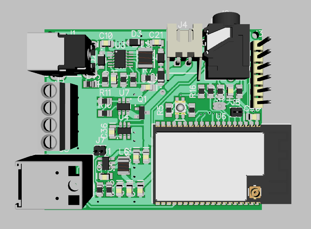
- Espressif's WROVER board based on ESP32 WiFi/BT chipset (built-in antenna)
- WiFi / BT connectivity
- TI's TAS575x stereo class-D amplifier for up to 2x20W (careful with heat dissipation)
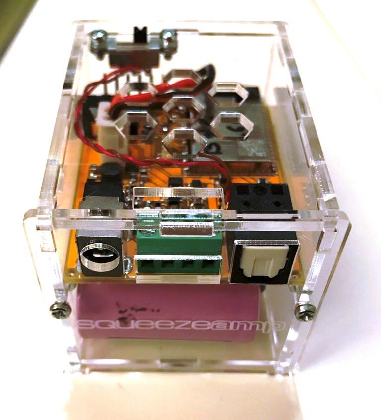
- Built-in battery charger (2 or 3 Li-Ion cells in serie) and automatic switch between battery and main
- Direct speaker output
- Jack 3.5mm for analogue line-out (with insertion detection) ==> <strong>this NOT supposed to be a headset output but it seems to drive enough for small 3 pins headphones at decent volume (need to check)</strong>
- SDPIF optical output
- Connector for 5/8 extra general purpose I/O (SPI, I2C, I2S, GPIO ...) ==> can add screen, buttons, rotary encoder ...
- 2 pins (1.27mm) on/off header (off mode consumes about 0.3mA on battery, a few tweaks can bring it down to 0.1 mA)
- 2 pins (1.27mm) GPI/sensor header (see ESP32 documentation about sensor_vn and sensor_vp)
- 6 pins (2.54mm) header provide 3.3V (output), GND, reset and serial flash download (boot, rx, tx - which can be reused at general purpose IO)
- 2.5mm Power Jack with Vcc 5...16V (20V under certain conditions see note on power supply below)
- A/D for Vcc measure
- Charge LED, bi-color LED
Looking at the board, TOP refers to the side that has the WROVER module and LEFT is where the Power Jack is located
What can it do
With the squeezelite-esp32 software, you can
- Stream from LMS and send audio to the build-in amplifier, the line-out jack, the spdif connector or another bluetooth speaker. You can also use an external I2S DAC if you connect it to the general purpose 5/8 pins connector and tweak the software. Synchronization works.
- Stream from a Bluetooth device and send audio to the same outputs, except of course for sending to another bluetooth speaker ... There is no guarantee of audio/video synchronization at this point
- Stream from an AirPlay1 device (iPhone, iTunes ...) to the same outputs, including to a bluetooth speaker. Synchronization works.
- Add your own buttons (no rotary encoder yet) and map/combine them to various functions (play, pause, volume, next ...
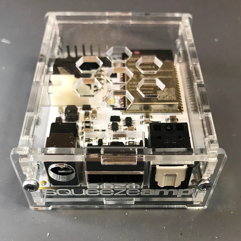
- Add a display like this one which can be directly connected to the 6-pins headers on PCB 3.x. Currently, only SSD1306-based displays are supported and for LMS only.
Tools, source and BOM
I'm using diptrace for schematics and routing which is free up to 300 pins. I had to do a few custom components and patterns, let me know if they are missing or if you cannot use the free version, I'll try to do some export to other PCB formats if needed You can order the PCB directly from PCBway here There is an excel file with is the BOM extract from diptrace and another one that points to all components from DigiKey The WROVER documentation can be found on Espressif site Download tool is here
Connectors & WROVER pin assignments
There are 3 PCB version, with a basic and a boost option for each one (see below for basic/boot differences).
All connectors are through-holes so that you can not populate them and directly solder wires if you want to use the board inside another equipment (Under parenthesis is the WROVER pin number).
- J1: power jack
- J2: audio jack
- 4: (6 - IO34) Detect ==> has pull-up and should be set to ground to detect jack insertion
- J3: main header
- PCB 1.x and 2.x
- 1: GND
- 2: EN/reset (3) ==> connect to RTS if possible
- 3: 3.3V output
- 4: Boot (25) IO0 ==> pull down at reset to enter download mode (connect to DTR if possible)
- 5: RX (34) IO1
- 6: TX (35) IO3
- PCB 3.x and above
- 1: GND
- 2: 3.3V output
- 3: RX (34) IO1
- 4: TX (35) IO3
- 5: EN/reset (3) ==> connect to RTS if possible
- 6: Boot (25) IO0 ==> pull down at reset to enter download mode (connect to DTR if possible)
- PCB 1.x and 2.x
- J4: battery connector
- 1: +
- 2: -
- J5: speaker connector
- 1: L+ (square pad)
- 2: L-
- 3: R-
- 4: R+
- J6: IO extension connector (note that a right-angle and a straight versions exist)
- PCB 1.x and 2.x
- 1: (26) IO4
- 2: (29) IO5
- 3: (30) IO18
- 4: (31) IO19
- 5: (33) IO21
- PCB 3.x and above: added pins
- 6: (35) IO2/GND depending on S2
- 7: (36) IO22
- 8: (37) IO23
- PCB 1.x and 2.x
- J7: on/off (on when floating/open)
- 1: GND
- 2: ENable ==> short with pin 1/GND to switch off 3.3V power
- J8: Input/Sensor connector
- 1: (5) IO39
- 2: (4) IO36
- S2: boot switch on 1.x and 2.x and select J6 pin 6 between GND and IO2 on 3.x
- Green LED: (14) IO12, active low
- Red LED: (16) IO13, active low
- TAS575x Speaker mute (13) IO14
- TAS575x Speaker fault (24) IO2
- TAS575x SCL/SDA: (11) IO26 / (12) IO27
- TAS575x I2S WS/SD/CLK: (10) IO25 / (8) IO32 / (9) IO33
- SPDIF: (23) IO15
<strong>Note that is no reverse polarity protection on the battery pins, so be careful as it will toast the power switch TPS22810 and probably the PCB itself. There is polarity protection on the main.</strong>
Flash download & operation
For at least initial download, you need a serial connection with ideally RX/TX/RTS/DTR and at least RX/TX. There is no build-in converter.
Connect RX/TX to J3 pin header. If you don't have DTR/boot, set the boot switch underneath (onPCB before 3.x) and if don't have RTS/reset, press the tiny reset button. After PCB 3.x, you must connect DWL to ground while resetting (simply put a wire on pin 6 of J3 and connect it to any ground)
The esp32 will enter download and you'll be able to update the software, as described on the squeezelite-esp32 site. This procedure is rarely needed as the software supports OTA update.
Don't forget to flip again the boot switch if you used it and the reset the board (or have the espressif tool do it for you), then follow the instructions here or have fun with your own software
Populating options
System is modular and you can pretty much build each sub-part independently.
If you don't want battery, don't populate charger, undervoltage detection and power OR and boost (on the boost option, see below). This is all top upper and middle right & left side of the PCB. You can short the large Schottky diode on the bottom side, but I recommend you keep it just in case.
If you don't want the amplifier, don't populate the bottom side, except for the power diode and the optical connector's decoupling capacitor (if you want SPDIF optical). In that case, note that the analogue output will not be available.
The SPDIF is always available, it just requires the WROVER module (which should at least always be here ...).
The battery connector is the angled version of the classical short 2 pins JST. You can use a longer version if you want the pins to extend a bit beyong the PCB (like the jack connector). You can also use a vertical connector here
Power options
I've been through a lot of back and forth about power. To charge 3-LiIon cells, the LT3652 requires at least 16V (Vbatt + 3.3V). But when powered with 16V, the TAS575x produces a fair bit of heat while it almost does none at 12V. Similar, the original design charging rate was 1A, but that got the LT3652 and inductor super hot, so I've reduced is to 0,66A (8W max). The rate is 0.1/R7 so you can tweak it if you want, on paper the design is capable of 1A.
When using 2 cells, a 12V power supply is sufficient which is ideal for the TAS575x, but then when used on battery the audio power is much less as the battery will provide 6~8.4V. Charging rate in that case is 0.75A.
So finally, I have 2 PCB options, the boost being the most versatile one but the most expensive as well. If you decide to not populate the battery charging, you can skip the rest of that section.
Basic design
2 cells mode is the simplest option. Power supply can be 12-20V, but 12V is recommended to optimize heat dissipation unless you want maximum amplifier power.
In 3 cells mode, the power supply must be 16-20V and a few components must be changed
- R8 (412k) ==> 340k
- R9 (634k)==> 953k
- R11 (25.5k) ==> 15.8k
- D5 (2.4V Zener) ==> 5~8V Zener (I use 5.1)
- R7 (0.13) ==> 0.16
In both case, if you limit the power supply to 16V, you can use 25V for all capacitors which saves a fair bit of cost for the 22µF. It does not change anything for others (indeed 50V can a be cheaper option for 100nF for example).
Boost design
This PCB option include a boost converter so that power supply can be 12V even in 3 cells modes. With that, the TAS575x is always powered with ~12V which is the ideal ratio heat/amplifier power. The boost converter will up the power supply to comply with LT3652 requirement of Vcc > VBat + 3.3V
The values of R8, R9, R11, D5 and R7 need to be set per values above if you chose 3 cells. If you want to use 2 cells, it's better to change the boost feeback resistors R12 and R18 to produce 12V only, but it's not mandatory. I don't think that using boost and 2 cells makes lots of sense, better just use basic and 12V then.
If you use that PCB and don't populate the boost converter, you can put a shunt directly between D2 and D7 anode and cathode. But then the LT3652 charger is not protected against polarity inversion ... to fix that, as D2 and D7 are separated by enough space, you can use a 0805 diode like this one ... your choice.
Understand that boost option produces more heat when charging the battery. It's inherent to the cumulated efficiency losses by boosting up Vcc then switching it down to charge battery. You might prefer to use the basic option which produces more heat on the amplifer instead. There is no perfect option.
When disconnecting main power, the battery should kick-in without interruption, but there might be cases when playing at high volume where combination of switch/capacitors will not store enough energy (un-plugging the connector creates many bounces, it's not a clean cut). This does not happen with the basic version because the power OR will always feed the system and main is 3.3V above battery. In the boost version, the power OR is not enough to select the right source as the main voltage is a bit below the battery voltage (and we don't want battery to feed the system when plugged on main), so the undervoltage switch is re-used to disconnect the battery when main is plugged. But the control of that switch might not act as fast desired. You can add a large electrolytic cap anywhere after the battery and main power OR.
The comment on capacitor voltage ratings apply as the boost is 16V only, so 25V works as it is below Vcc * 1.45
Versions
Version 2.x uses the TAS578x instead of TAS575x.The PCB change is tiny but critical as TAS578x has a reset pin that must be pulled high (direct Vcc connection, no room for a proper pull-up resistor) otherwise it does not boot. Normally, version 2.x can be used with TAS575x, providing that the TAS578x reset pin which is a GPIO in TAS575x is not driven low.
Version 3.x expands the J6 5 pins I/O connector to 8 pins and changes S2 slide switch function to select pin 6 of this connector to be either ground or GPIO2. The 6 pins header is reshuffled to allow of an OLED display without wires.
The benefit of changing J6's pin 6 to GND is, for example, to bring a GND wire to a button expansion board of your own. There is no need of Vcc as the ESP32 has optional pull-up. Still, if you want a Vcc, you can use one GPIO as a supply, with a maximum of 40mA per pin.
(Executive) Summary
- don't want battery, use the basic version and maybe do not populate all the charger-related components
- want to minimize heat: use 12V
- want maximum audio power: use up to 20V
- want battery
- don't need too much audio power when battery powered: choose basic (2 cells) and power it with 12V.
- want more audio power:
- don't care much about amplifier's heat: choose basic (3 cells) and power it with 16+V (put a sink on the TAS575X and the exposed pad).
- want to minimize amplifier's heat, choose boost (3 cells) and power it with 12V
- want simply to power with less than 12V, choose boost (2 or 3 cells).
Limitation & Disclaimer
This contains a power amplifier and a charger on a small board, so it gets pretty hot when used at high power. I've added a small exposed copper area where you can add a heatsink and also use a fan to help cooling down, but I cannot guarantee that this design works well and safely with continuous high volume. My own use is at moderate volume.
Similarly, the charger is for Li-Ion and such cells have inherent safety issues. It's using a LT3652, which is a good charger that takes care of battery maintenance, but there is no thermal management, so be careful and ALWAYS use protected Li-Ion cells. There is battery undervoltage detection on board so that the systems shuts off when battery voltage is too low. There is no under voltage detection for main supply.
<strong>This is by no mean a professional design so use it at your own risk. I will not be liable for any issue caused by that board</strong>. I'm making it public in case somebody with enough knowledge will find it useful, so know youwhat 're doing first. Similarly, this is not an audophile design, so please do not complain or ask me for some linear power or 32 bits / DSD insanities. The SqueezeESP software can do 16 bits @ 192 kHz which is way more than enough, in fact 48kHz/16 should be sufficient.